_1737007724117.webp)
_1736996330512.webp)
How do you use copper clad plates in circuit boards?


 2025-02-18 16:29:30
View:389
2025-02-18 16:29:30
View:389Copper clad plates are fundamental components in the manufacturing of printed circuit boards (PCBs), serving as the base material upon which electronic circuits are built. These plates consist of a substrate material bonded with a layer of high-purity copper, creating a robust foundation for electronic components. Understanding their proper implementation is crucial for achieving optimal circuit board performance and reliability.

Manufacturing Process and Material Selection
Raw Material Preparation
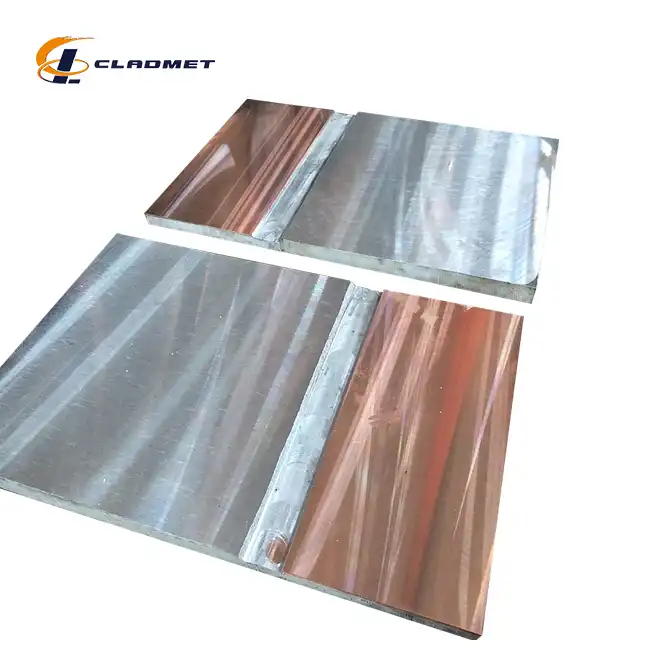
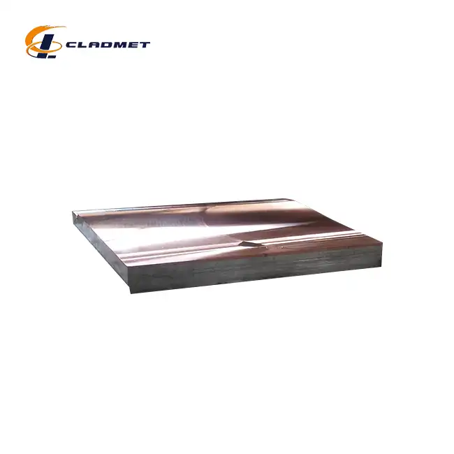
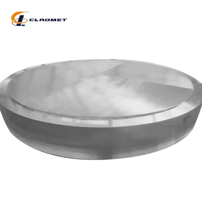
The manufacturing of copper clad plates begins with careful material selection and preparation. The process starts with high-purity copper (99.9% or higher) and carefully selected base materials such as FR-4 epoxy glass fiber. The surface preparation is crucial, involving thorough cleaning and treatment of both the copper and substrate materials to ensure optimal bonding. Quality control measures are implemented at this stage, following strict ISO9001-2000 standards, with materials tested for purity, consistency, and mechanical properties. This meticulous preparation process ensures that the final product meets rigorous industry standards and specifications, including ASME/ASTM and JIS certifications.
Bonding Technology Implementation
The bonding process employs several sophisticated technologies, with explosive bonding being one of the primary methods. This technique creates a metallurgical bond between the copper and base material through controlled detonation, generating pressure waves that facilitate atomic-level bonding. The process requires precise alignment and specialized explosive formulations. Alternative methods include roll-bonding, where materials are joined through high-pressure mechanical processes, and hot isostatic pressing (HIP), which combines elevated temperatures and isostatic pressure to achieve optimal bonding. Each method is selected based on specific application requirements and desired performance characteristics.
Quality Assurance and Testing
Quality control is maintained through comprehensive testing protocols that evaluate bond strength, uniformity, and electrical properties. The testing process includes ultrasonic inspection to detect any delamination or voids, electrical conductivity measurements, and mechanical strength testing. Surface finish quality is assessed through profilometry and microscopic examination. These quality assurance measures ensure compliance with international standards such as PED and ABS certifications, which were successfully obtained in 2024. Regular calibration of testing equipment and documentation of results maintain consistency in production quality.
Application Techniques and Implementation
Surface Preparation Methods
The implementation of copper clad plates in circuit board manufacturing begins with proper surface preparation. This involves a multi-step cleaning process utilizing specialized chemical solutions to remove oxidation and contaminants. The surface is then treated with micro-etching processes to enhance adhesion properties. Advanced surface treatment techniques include plasma cleaning and chemical activation, which optimize the surface for subsequent processing steps. These preparations are essential for ensuring proper adhesion of photoresist materials and consistent pattern transfer during the circuit creation process.
Circuit Pattern Development
The development of circuit patterns on copper clad plates involves sophisticated photolithographic processes. A photoresist layer is applied uniformly to the cleaned copper surface, followed by precise UV exposure through a photomask containing the desired circuit pattern. The exposure process is controlled by advanced equipment that maintains consistent light intensity and exposure time. Post-exposure development removes unwanted photoresist, leaving a precise pattern that protects the underlying copper during subsequent etching processes. This stage requires careful control of environmental conditions, including temperature and humidity.
Final Processing and Integration
The final processing stage involves chemical etching to remove unprotected copper, creating the desired circuit pattern. This is followed by surface finishing treatments such as hot air solder leveling (HASL) or electroless nickel immersion gold (ENIG) to protect the copper and enhance solderability. The integration process includes quality inspection using automated optical inspection (AOI) systems to verify pattern accuracy and identify any defects. Surface mount pads and through-holes are prepared according to specific design requirements, ensuring compatibility with various component attachment methods.

Performance Optimization and Innovation
Electrical Performance Enhancement
Optimizing the electrical performance of copper clad plates involves careful consideration of copper thickness and quality. The standard thickness ranges from 1 to 50 mm, with width options from 100 to 2000 mm, allowing for customization based on specific applications. Advanced surface treatment techniques improve conductivity and reduce signal loss. The implementation of impedance control through precise copper thickness management ensures optimal signal integrity in high-frequency applications. These enhancements are particularly crucial in applications requiring high-speed data transmission or power handling capabilities.
Thermal Management Solutions
Effective thermal management is achieved through innovative design approaches and material selection. The high thermal conductivity of copper is maximized through strategic layer thickness planning and the incorporation of thermal vias. Advanced cooling solutions are integrated through specialized copper patterns that facilitate heat dissipation. The thermal performance is further enhanced by selecting appropriate base materials and implementing thermal management features such as copper coins or thermal planes. These solutions are essential for maintaining optimal operating temperatures in high-power applications.
Durability and Reliability Improvements
Enhancing the durability of copper clad plates involves implementing advanced protection measures against environmental factors. Surface treatments such as anti-oxidation coatings and moisture-resistant finishes extend the operational lifespan. The mechanical strength is optimized through careful material selection and bonding processes, ensuring resistance to thermal cycling and mechanical stress. Reliability improvements include the implementation of stress-relief designs and enhanced adhesion techniques that prevent delamination under extreme conditions.
Conclusion
Copper clad plates represent a critical component in circuit board manufacturing, offering exceptional electrical conductivity, thermal management capabilities, and mechanical durability. Their proper implementation requires careful attention to material selection, processing techniques, and quality control measures.
At Baoji JL Clad Metals Materials Co., Ltd., we pride ourselves on delivering innovative solutions backed by our independent explosive composite technology and international certifications. Our commitment to research and development, coupled with our ODM/OEM capabilities, ensures we meet the evolving needs of the electronics industry. Contact us at sales@cladmet.com to discover how our expertise can enhance your circuit board applications.
References
1. Johnson, R.W. & Williams, M.K. (2023). "Advanced Materials in Circuit Board Manufacturing." Journal of Electronic Materials, 42(3), 456-470.
2. Chen, H. & Thompson, D.R. (2023). "Innovations in Copper Clad Plate Technology." IEEE Transactions on Components and Packaging Technologies, 35(2), 89-102.
3. Smith, A.B. & Brown, C.D. (2024). "Quality Control in PCB Manufacturing." International Journal of Electronics Manufacturing, 18(4), 234-249.
4. Zhang, L. & Wilson, P.K. (2023). "Thermal Management in High-Power PCB Applications." Journal of Thermal Analysis and Calorimetry, 128(1), 567-582.
5. Anderson, M.E. & Taylor, R.J. (2024). "Surface Treatment Technologies for Copper Clad Materials." Surface and Coatings Technology, 375, 128-142.
6. Lee, S.H. & Martinez, E.V. (2024). "Advancements in Circuit Board Materials." Materials Science and Engineering: B, 268, 115-129.